Search
NEWS

Schematic of the chip/bump build-up cross-section.

By A Mystery Man Writer

Schematic of the chip/bump build-up cross-section.

Chip Bonding - an overview

Schematic of the chip/bump build-up cross-section.

Thermal copper pillar bump - Wikipedia

Schematic of the chip/bump build-up cross-section.

Electronics, Free Full-Text

Schematic of the chip/bump build-up cross-section.

Levels and Steps of Integration. Introduction, by Suny Li

Schematic of the chip/bump build-up cross-section.

Basics of chip/package codesign in a large flipchip application

Schematic of the chip/bump build-up cross-section.

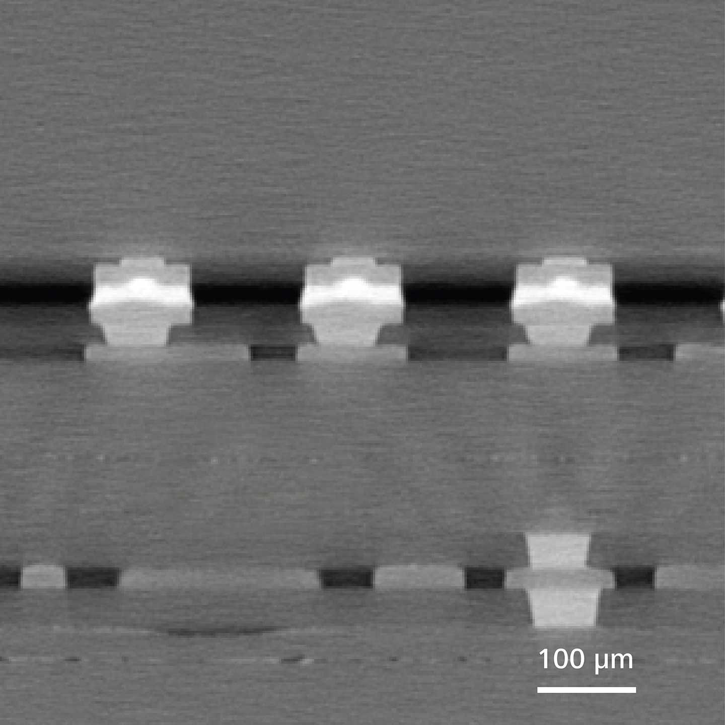
SEM image of a cross section of an unstressed 30 μm solder bump

Schematic of the chip/bump build-up cross-section.

Cross-section of solder bump (a) and package structure of flip

Schematic of the chip/bump build-up cross-section.

Ball grid array patented technology retrieval search results

Schematic of the chip/bump build-up cross-section.

Schematic of the chip/bump build-up cross-section.

Schematic of the chip/bump build-up cross-section.

Polymers in Electronic Packaging: Semiconductor Substrates for

Schematic of the chip/bump build-up cross-section.

a) Schematic of 3-D stack package. (b) Cross section of 3-D stack

Schematic of the chip/bump build-up cross-section.

Faraday Technology Corporation-Flip-Chip Package

Schematic of the chip/bump build-up cross-section.

Schematic of the chip/bump build-up cross-section.

Schematic of the chip/bump build-up cross-section.

Microscopy Solutions for Advanced Semiconductor Packaging

Schematic of the chip/bump build-up cross-section.

Cross-section of solder microbump on the Si chip (not in scale) (a